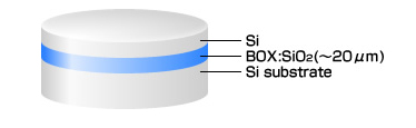
SOI Wafer
SOI Wafer of SEIREN KST
SOI(Silicon on Insulator)Wafer is a silicon wafer which is a structured single crystalized layer on oxidized layer and used in the field of high speed LSI, low power LSI, powerdevice, MEMS.
Except for normal SOI, we provide special SOI wafer such as Cavity SOI wafer or Thick BOX SOI wafer.
Cavity SOI will be a good performance on reducing process steps or yield loss, and this would be the possibility for reducing huge cost cutting.
Also, Thick BOX SOI wafer is made by KST’s unique super thick thermal oxidized layer technique which has never been existed before, and possible to make silicon photonics, or super high resistivity powerdevice in the world.
Capability
| Size | 6” 8” |
|---|---|
| Device layer thickness | 100nm※~200μm |
| Wafer in Wafer thickness accuracy | Thin layer ±15nm Thick layer ±0.5μm |
| BOXlayer thickness | Maximum 20μm |
※ Thin thickness device layer products is a corroborated products which is manufactured with Shin-Etsu who has a thin device layer making technology and KST’s thick oxidized technology combined together.
We can make a handle wafer thickness as >=350um.
We can do a pattern process on a Device layer Wafer・BOX layer・handle Wafer
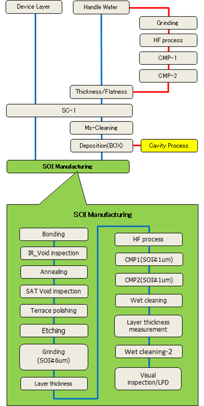
After bonding, we manufacture the SOI wafer one by one so that we can customize them in several varieties and in a few quantities. KST can manufacture 1um as minimum thin device layer.
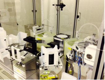
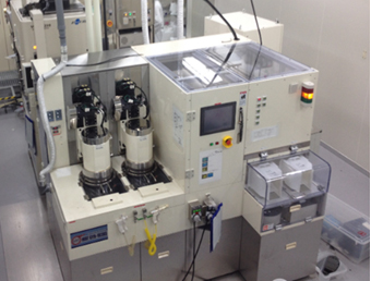
Main Equipment
Bonding tool
Grinding tool
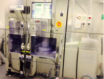
CMP tool
Introduction of variety of SOI wafer
Normal SOI…
General SOI which is structured by Device layer / BOX/ Handle wafer.
We can correspond on other than 3 layered SOI such as SOI-1.
Cavity SOI…
There are cavities inside of the SOI and there will reduce the Backend processing after dicing and it will be expected to be many products.
Thick-BOX® SOI…
SOI wafer which has thick BOX 3~20um. It will be effective for high resistivity material.
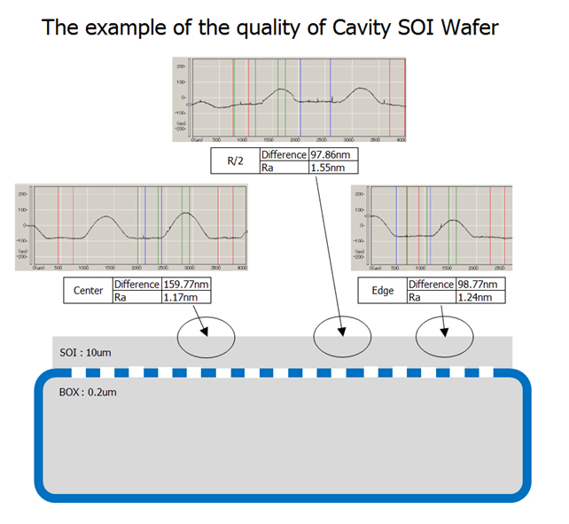
SOI wafer Cavity SOI…
Cavity SOI
Cavity SOI wafer is one of the SOI wafer which has cavities or patterns inside of multi-layered wafer. It will reduce several processes after a dicing process, and it will be expected to become many products. We can process the cavity structure not only on handle wafer but also on BOX layer, and we can customize as per customer’s requests.
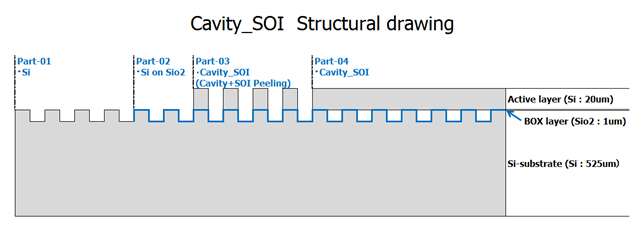
※The above structure is an example case which is processed on a handle wafer.
We can process on BOX layer, or any other and so on, as we wait for your inquiries,
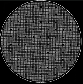
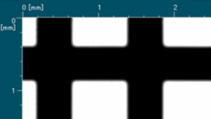
Ultra sonic voids measurement on Cavity SOI
SOI Wafer Thick-BOX® SOI…
Thick-BOX® SOI
The Thick-BOX® SOI wafer is a thick BOX structured SOI wafer which has been manufactured by KST’s unique super thick oxidized layer technique.This has been used for super high resistivity semiconductor power devices.
Also, this is effective for a bulk type MEMS which does etching processing on BOX layer such as acceleration sensor or actuator and so on. By making a thick BOX layer as sacrificed layer, a structured part can be moved smoothly and can take enough space, and it will be solve in a sticking problem and the movement range will become wider to the horizontal. It will be accomplish for the better yield rate and the idea of new device R&D.
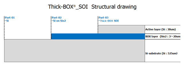
※The above mentioned combination of a handle layer and a device layer is one of the example.
We can customize any thickness of structures. We are looking forward to receiving your inquiries.
Example of the use of Thick-BOX® SOI Wafer
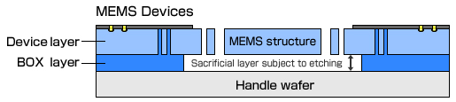 ※MEMES structure part, Sacrifice layer etching part
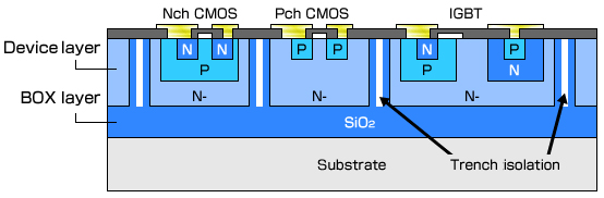
※Power Device “IGBT”