Process Service・Test Wafer
We will offer a variety of deposition processes and various films with wafer of research and development applications involved in the semiconductor manufacturing process.
Rich processing menu of specialized manufacturer unique will meet the various needs of customers.
In addition, its own super-thick thermal oxide film formation technology is the material that is essential
to the optical device to support the optical communication.
Our products and technologies have been adopted to communication equipment
manufacturers and optical component manufacturers worldwide.
Process Line-up
| Type | Method | Film Type |
|---|---|---|
| Thermal Oxide | Thermal Oxidation | Thin thermal oxide film |
| Super-thick thermal oxide film | ||
| LP-CVD | LP-SiO2 | |
| HTO | ||
| LP-TEOS | ||
| PE-CVD | PE-SiO2 | |
| PE-TEOS | ||
| HDP | ||
| Low-k(BD、BDⅡ、AURORA、CORAL) | ||
| PSG | ||
| NSG | ||
| BPSG | ||
| Spin-coated | SOG | |
| Annealing oven | RTO | |
| Nitride | LP-CVD | LP-SiN |
| PE-CVD | PE-SiN | |
| Si | LP-CVD | Poly-Si |
| Amorphous-Si | ||
| Organic | Spin-coated | G-Line resist |
| I-Line resist | ||
| KrF resist | ||
| ArF resist | ||
| Polyimide(Photosensitive、Non-Photosensitive) | ||
| Metal | Sputter | Al、Al-Si、Al-Si-Cu、Al-Cu |
| Ti、TiN | ||
| Ta、TaN | ||
| Cr | ||
| Cu | ||
| W | ||
| Ni | ||
| Au | ||
| Pt | ||
| ITO | ||
| Plating | Ti、Ni、Au、Cu | |
| CVD | W-Si |
※There are also things that can’t be processed by the wafer size.
※In addition, because the other films can also, please say a hope. Please contact us for details.
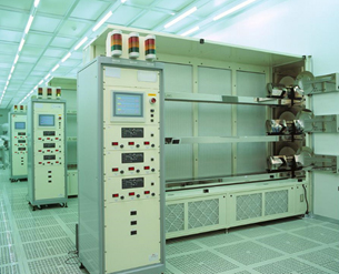
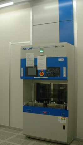
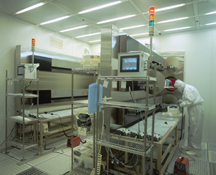
| Our Clean Room | |
 |
 |
 |
|
Process Service
“Super-thick thermal oxide film” applications
Undercladding wafer for AWG
With respect to optical waveguides (AWG), the so-called undercladding layer, which is the lowermost SiO2 film, has a critical effect on the process yield.The Super-thick thermal oxidized films of KST World have the leading share of the global market thanks to their excellent surface cleanliness and stable film quality.
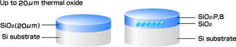
Guaranteed specifications
| Item | Specification |
|---|---|
| Film thickness | 20um±5%(Maximum thickness) |
| In-plane uniformity | ±0.5% |
| Surface uniformity | ±0.5% |
| Refractive index(@1550nm) | 1.4458±0.0001 |
Standard product line-up
| Size | Wafer thickness | Thermal oxidized film thickness |
|---|---|---|
| 4 inches | 525um 1mm | 15um、20um |
| 6 inches | 625um 675um 1mm | 15um、20um |
| 8 inches | 725um | 15um、20um |
| 12 inches | 775um | 15um |
※The above wafer size and thickness, are described our standard products.
※Other sizes and thicknesses are also available. (Up to a maximum thickness of 30μm)
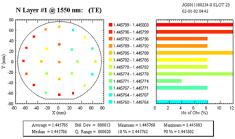
Refractive index plane distribution data
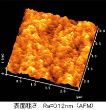
Surface roughness data